Semiconductor PLM and MES for the UK
Precision at scale — maximising yield in the world's most demanding manufacturing environment
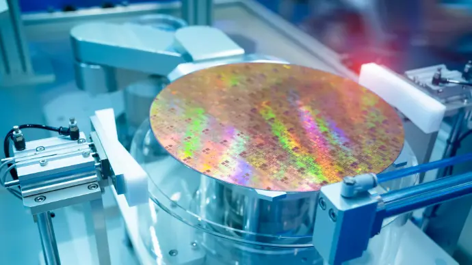
Semiconductor manufacturing operates at tolerances measured in nanometres, where a contamination event can destroy millions of pounds in product. We help fabs facilities optimise yield, reduce cycle times, and build the digital infrastructure needed to compete in a capacity-constrained market.
The Semiconductor Landscape
Yield Improvements
Through advanced process control and integrated system connectivity
Less Downtime
Through planned and preventative maintenance activities
Faster Ramp-Up
Reduction in process and production ramp-up time when using pre-integrated partner solutions
Pains Holding You Back
The industry's combination of extreme precision, massive capital investment, and relentless technology evolution creates unique pressures.
Nano-Scale Transformation
Implemented comprehensive Manufacturing Discovery Program addressing systemic Product, Process and Production inefficiencies. Achieved 90% yield, 100% stakeholder collaboration, and implementation of a structured methodology Process FMEA.

Gains You Make With Us
Practical solutions for organisations where nanometres matter and minutes of downtime cost millions.
-
 Run-to-run control optimisation
 -
Fault detection & classification (FDC)
-
SPC & process capability analysis
-
Equipment health monitoring
-
Predictive maintenance models
-
Spare parts optimisation
-
Wafer-level yield mapping
-
CAPA management systems
-
Defect Pareto & root cause analysis
-
SEMI integration (SECS/GEM, EDA)
-
Data lake architecture
-
Real-time dashboarding
-
WIP flow optimisation
-
Bottleneck identification
-
Lot prioritisation systems
-
Traceability & lot genealogy
-
Customer audit preparation
-
FMEA & control plan management
FAQs
Common questions UK semiconductor manufacturers ask about working with TJ Digital Systems
Do you work with UK semiconductor manufacturers?

Yes - we work with UK semiconductor operators on the manufacturing systems side: PLM (via CIM Database from CONTACT Software), MES, quality systems and manufacturing assessment. We focus on general manufacturing infrastructure, not on cleanroom-specific equipment integration such as SECS/GEM. For specialist fab equipment integration we partner with sector specialists.
Can the UK still build a competitive semiconductor manufacturing base?
Yes, particularly in compound semiconductors, photonics and specialist analog or mixed-signal where the UK has historic strength. Centres like the Compound Semiconductor Applications Catapult in Newport and the photonics cluster around Cambridge and Glasgow show that the UK is competitive in the segments where it specialises.
What does TJ Digital Systems bring to UK semiconductor manufacturers?
We bring the manufacturing systems layer: PLM for product and process documentation, MES for production tracking, quality systems and a manufacturing assessment approach that finds the highest-impact improvements quickly. We pair our hands-on UK manufacturing engineering experience with CONTACT Software’s PLM platform.
Where does TJ Digital Systems’ expertise end in semiconductor manufacturing?
We are upfront: we know general manufacturing systems and processes. We are not a specialist fab consultancy and we do not do photolithography or SEMI-specific equipment integration as a primary offering. Many of our UK semiconductor clients use us for the systems layer alongside specialist partners for the cleanroom side.